Without
doubt the most important development in microwave technology during the
last decade has been the Monolithic Microwave Integrated Circuit (MMIC).
The MMIC is to the RF engineer what the integrated logic gate was to
the computer engineer, decades ago - the means of building complex
designs with economical prepackaged functional blocks. In this month's
feature we will take a closer look at the MMIC and its implications for
microwave and digital communications over the coming years.
RF Design Issues
Designing analogue hardware to operate at radio
frequencies (RF) has traditionally been a relatively messy process, in
comparison with digital logic design, and remains very much the domain
of a very specialised community of engineers. RF hardware is by its
basic nature analogue, and few opportunities existed in the past
practice of the design process to abstract functional blocks and avoid
the frequently pathological behaviour of component level designs.
Let us consider a sixties or seventies RF design such as
a low noise preamplifier used in a receiver. The available component
base comprised primarily Silicon and Germanium bipolar transistors,
axial lead resistors and capacitors, and ferrite and air core inductors.
Each and every one of these components exhibits
parasitic or stray capacitance, inductance and in the transistors,
internal capacitances resulting from the geometry of the transistor die,
and the behaviour of the semiconductor junctions.
A design engineer would therefore construct a fairly
elaborate mathematical model for the intended circuit's behaviour in the
RF domain, and concurrently would also have to do the same for the
direct current (DC) behaviour of the circuit to ensure that the
transistor was operating in the intended regime and was stable with
varying temperature. To complicate things, a noise performance model was
also required, to account for the thermal noise in resistors and shot
noise in the transistor. Of course, calculations or simulations would
also be required to account for component tolerances, since RF
transistor specs would be very loose, and 1% accurate resistors rather
expensive.
Through repeated iterations using a calculator, or if
paid for by a serious employer, a software simulator like SPICE, the
engineer would zero in on the intended combination of component values
to get the right balance between gain performance, noise performance and
thermal stability, while looking over his shoulder for the company
accountant, heard mostly complaining about project delays and
extravagant choices in transistors and capacitors.
Once the theoretical design was completed, a prototype
would be fabricated on a printed circuit board and tested. No chance of
delegating the printed circuit board layout to a draftsman since the
oddities of RF require that the primary designer produce the layout him-
or herself.
Usually the prototype would oscillate due to feedback
coupling at radio frequencies, and would require revisions to the board
layout and judicious adjustments in component values, mostly determined
empirically yet again through multiple iterations. Finally a working
prototype existed.
The next phase in the process was a demonstration
production unit, built to the documentation package in a production
environment and carefully tested to verify its performance. More than
often further iterations would follow.
Finally, the design would be transfered to production,
and would usually require manual adjustment by a technician to exactly
meet the intended specification. Very careful and accurate assembly was
mandatory, to ensure that parasitic inductances and capacitances were
not inadvertently added into the design by cutting component leads to
the wrong length, or putting a bend in the wrong spot.
Was this messy ? Absolutely !
Classical RF design and manufacture was time consuming
in every respect, during every portion of the process from idea to end
product. Increasing the operating frequency from the HF, VHF to UHF was
a headache, and going microwave a nightmare. At microwave frequencies,
even tiny stray capacitances of nanoFarads and inductances of
nanoHenries could wreak havoc with a design. Moreover, shielding covers
or cavities to contain the circuit would contribute.
Perhaps the biggest headache of all was reproducibility
in designs, since the combination of sloppy component tolerances and
mechanical assembly left many opportunities for designs to deviate from
the intended specification.
By the seventies RF designers with the budget to do so
shifted from printed circuits to hybrid circuits, using ceramic
substrates with resistors, capacitors and conductors fired on to the
surface of the ceramic substrate, and active components such as
transistors and diodes then soldered on to the substrate.
"Hybrids" proved to be excellent, since they allowed
much more compact physical designs, and tighter production tolerances.
Cost however remained a major issue, as a result of which hybrids became
a staple item in equipment like radars but continued to be a cost
problem for commercial and consumer equipment.
Another issue which proved to be an ongoing problem was
the performance of transistors with increasing frequencies. Silicon
bipolar transistors, the workhorse of the digital logic base, would
suffer worsening gain problems at several GigaHertz and were frequently
also noisy. While speed could be improved to a large degree by shrinking
the size of the transistor, a more subtle problem arose, which was
inherent in the Silicon material itself - poor electron mobility.
Mobility is a measure of how quickly charge carriers
(electrons, holes) can travel in the crystalline lattice when an
electric field is applied. The lower the mobility, the stronger the
field required to make them move quickly. In a transistor which is
trying to amplify a signal at many GigaHertz, poor mobility tranlstaes
into poor gain, and gain is the measure of a transistor's worth in most
of its uses.
The answer was to be found in GaAs semiconductors,
rather than Silicon. GaAs has typically around six times the electron
mobility of Silicon, providing the potential for significantly faster
transistors. GaAs also proved to be better from a noise performance
perspective, so the two key problems in an RF transistor, speed and
noisiness, were ostensibly solved by the GaAs transistor.
The reality was not as tidy as was initially expected.
It has taken almost two decades for GaAs components to transition from
the early production components to today's mature volume products.
During my undergraduate years, the standard joke in the EE community was
"GaAs - the material of the future - still ...".
The problems with GaAs were manifold. The material
proved to be very difficult to fabricate, the transistors proved to be
very fragile and easily damaged by electrostatic discharge, overheating
or electrical overload, much more so than Silicon. In the employ of one
company, I was banned from using a GaAs transistor since it was expected
that the production workers could not solder them in without damaging
them !
The commercial pressures for more bandwidth grew very
rapidly during the early nineties, with the massive growth in mobile
telephone use, and the growth in the Internet. Mobile telephony proved
to the key volume driver for commercial commodity GaAs components.
However, the technology base for RF could not move ahead
while remaining shackled to Silicon integrated circuits and discrete
GaAs transistors.
Silicon fabrication techniques allow for digital
components which can be clocked well beyond a GigaHertz, and Silicon
allows for tremendous density. However, combining density with low noise
Silicon bipolar transistors has proven to be difficult, indeed the
fastest low noise Si bipolar discretes this writier has seen are only
useful to several GigaHertz.
Clearly the answer to this problem was to integrate many
GaAs transistors on to a single chip, in the manner performed with
Silicon successfully over the last 4 decades. This proved to be no mean
feat, given the finicky nature of GaAs as a material. The Microwave
Monolithic Integrated Circuit (MMIC - pronounced "mimic") proved to be
an elusive goal.
A lot of expensive research was required to push the
GaAs transistor from the domain of discretes into the integrated circuit
(IC).
Much of the early funding and early production of GaAs
ICs was paid for by the US DoD. They had a very strongly vested interest
in this respect, since radar remains the key military sensor used for
finding things to blow up. Whether we are building radars, or building
equipment to jam radars, we require high density, reliable, economical
RF building blocks. The particular prize in the military game was a
device called an Active Electronically
Steered Array (AESA), also known as a "phased array". An AESA is a
flat panel microwave antenna which can be pointed by individually
manipulating the phase shifts, or delays, of the hundreds or thousands
of individual receive and transmit elements which make up the array.
With no moving parts the AESA is very reliable, can
point its beam in milliseconds, yet it can be easily buried into the
flat surfaces of a stealth fighter or bomber, and can be built with
sidelobes 1/100 - 1/1000 the magnitude of a conventional mechanical
antenna. The AESA was the radar designer's dream.
The snag with the AESA is that it needs at least 1500
and more typically 2000 individual transmit receive modules, each of
which has to contain a transmitter, receiver and phase shifter, as well
as the radiating element, digital control bus and RF feed connections.
Operating at 10-20 GHz, each much be less than a centimetre in cross
section.
Needless to say the only technology which could possibly
allow the manufacture of the densely packed AESA TR modules was the GaAs
MMIC. The US DoD was the first major player, but quickly followed into
the fray by the EU and the Israelis, as well as the Japanese. All
funded research and pilot production, and now all are either paying for
the manufacture or the impending manufacture of AESAs.
Once the expensive research was done and the production
techniques were refined, the manufacturers quickly turned to commercial
applications, for which GaAs opened up huge possibilities: mobile
telephony, satellite telephony, mobile networking, multipoint
distribution, satellite communications. Any application which could
benefit from a RF chip using GaAs was a candidate.
The big attraction commercially lies not only in
performance, but also board level manufacturing, since economical high
volume robotic component placement can be used, and many of the
production tolerance problems seen with manual assembly simply go away.
The Silicon monolithic integrated circuit appeared
during the sixties and has since then revolutionised the computer
industry, as well as the consumer electronics industry. While the GaAs
MMIC is a late arrival, it promises similar revolutionary changes in RF
technologies, and many cabled high speed digital communications
technologies. Silicon will remain competitive in many lower speed RF
applications, but the high ground has now been taken by GaAs.
GaAs Transistors
The basic building block in any solid state integrated
circuit is the humble transistor, and this is no less true for a GaAs
MMIC. The transistor is used as a switch, an amplifier, or if contorted
in the right manner, a current source or load resistor.
In Silicon based technologies, the two "workhorse"
transistor types are the classical bipolar device, and the MOSFET, a
mainstay of high density digital circuits. Neither proved to be
practical for GaAs.
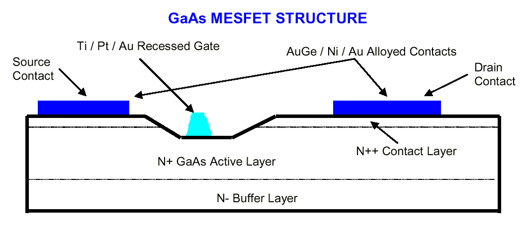
The first GaAs transistor to achieve high production
volumes, as individual disrete transistors, was the MESFET (Metal
Semiconductor Field Effect Transistor).
The MESFET is a close cousin to the Silicon MOSFET, and
like the MOSFET, is constructed with a source, gate, and drain (See
Figure 1. by Litton). A voltage change between the transistor's gate and
source pins causes a change in the current flow between the source and
drain pins. Unlike the MOSFET, where the gate is insulated from the
semiconductor substrate by an oxide layer, the MESFET uses a Schottky
metal junction produced by applying the metal gate electrode to the
semiconductor directly.
Unlike Silicon, where a MOSFET can be easily fabricated
by doping a source and drain, laying down an oxide for the gate, and
then putting down Aluminium connections for tracks, sources, drains and
gate electrodes, GaAs MESFETs are much more demanding to build.
The MESFET is fabricated on a GaAs substrate, using
Molecular Beam Epitaxy (MBE) techniques to grow extremely thin layers of
doped GaAs with precise thicknesses and compositions. The bulk of the
MESFET comprises a lightly negatively (N+) doped layer, over which a
more heavily doped layer is placed to form a base for the source and
drain contacts. Channels are etched into the substrate for the gates,
which are then applied as a layered Pt/Ti/Au (Platinum, Titanium, Gold)
structure and then carved to an exact trapezoidal shape using an
electron beam. The gate is about half a micron in length.
The source and drain contacts are then produced using
layered structures of Germanium gold alloy (GeAu), nickel and gold
(GeAu/Ni/Au), the Germanium doping the underlying GaAs to improve
contact performance.
While the MESFET provided a robust basic device for many
applications, especially those involving low noise high speed receivers
and buffers, its performance ceased to be competitive with the advent of
more complex High Electron Mobility (HEMT) transistors. MESFETs do
remain widely used, and are especially common in applications such as
switches and attenuators.
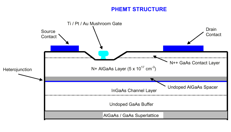
The HEMT (Figure 2. - Litton) transistor family spans a
range of devices, with manufacturers frequently using variations on the
nomenclature to label their proprietary flavour of the device.
Where HEMTs differ from older MESFET devices is in the
use of heterostructures, in which two different semiconductors are used
to form the transistor. While any meaningful discussion of the solid
state physics of GaAs HEMTs would exceed the scope of this treatment,
suffice to say that the heterojunction layer between the AlGaAs and
InGaAs creates conditions in which an electron gas with very high
mobility is formed. As a result the transistor is significantly faster
than the classical MESFET, which relies on the mobility performance of
the base material alone.
Pseudomorphic HEMTs (PHEMTS) are available with useful
performance out to many tens of GigaHertz.
GaAs MMICs
The step from the fabrication of individual transistors
to complete monolithic circuits with tens to hundreds of components on a
single slab of GaAs has its complexities. While the techniques for
processing the materials are essentially the same, quality demands do go
up since losing one transistor out of a hundred due to a fabrication
defect amounts to losing a whole chip die if you are fabricating a a
wafer of MMICs.
The other significant issue with MMICs is the
development of design rules for the layout of components and
connections, and the development of robust passive components such as
PIN diodes, resistors, capacitors and inductors which may be integrated
into the same slab of GaAs. Since the MMIC is a complete microwave RF
circuit on a chip, the design must reflect established RF design rules.
The density of a GaAs (or Si) MMIC is much lower than
that of competitive Silicon digital ICs, even if similar transistor
sizes are used, simply because of the need to observe the same RF design
rules which plagued RF circuit designers in decades past. Every track
is a waveguide ....
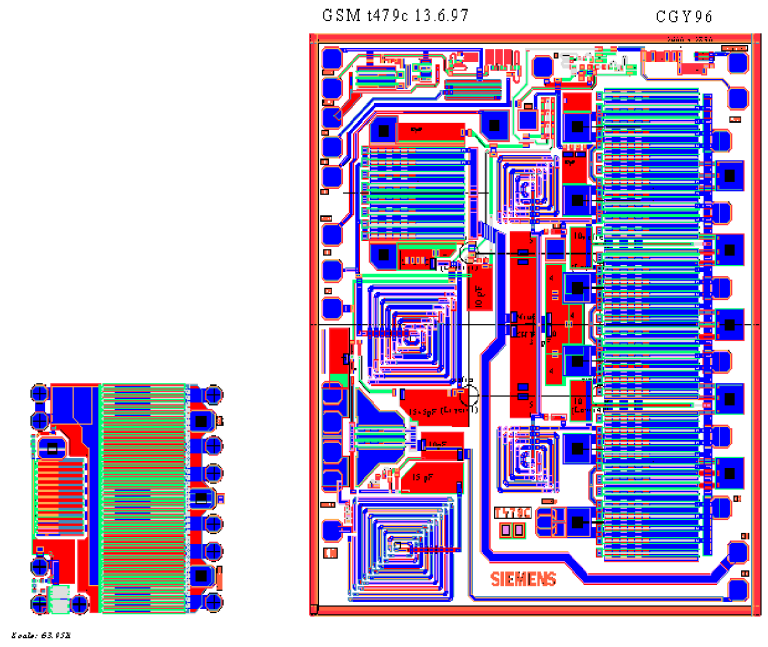
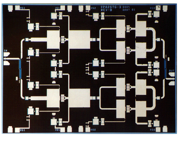
An example of a 60 GHz satcom power amplifier MMIC with
a 550 mW output rating (Lockheed Martin, Chao et al.) is depicted in
Figure 3, and a GSM MMIC (Siemens, Kapusta) is depicted in Figure 4.
Lower operating frequencies do allow some increases in density, but
millimetric band operation usually allows no compromises.
The great enabler for MMIC design has been the
availability of cheap compute power and excellent simulation software,
which allows engineers to devise circuits using previously tested
structures and frequently also building blocks.
A very wide range of GaAs MMICs are now available in the
commercial marketplace, many of which are general purpose building
blocks, some of which are versions of radar and AESA components, and
increasingly, custom devices for established commercial applications.
These devices can be supplied as dies alone for use in multichip modules
or hybrids, or in conventional resin TSSOP or SSOP28 packages for
robotic surface mount on printed circuit boards.
For a product designer working at the board level, a
suitable range of of-the-shelf MMICs allows the rapid design and
development of RF equipment with a minimum of fuss, since the most
difficult bits are hidden away in the MMIC. What we are seeing today in
RF design is what happened in logic design two decades ago, when MSI
chips largely changed the game.
Clearly the market for GaAs MMICs is booming, between
1997 and 1998 a 200-300% growth in deliveries was observed.
Manufacturers are now aiming at maximising volumes and minimising costs,
and have shifted from 4 inch wafers to 6 inch wafers. Cost still
remains an issue in comparison with Silicon, since the equipment for
molecular beam epitaxy and electron beam shaping is extremely expensive,
and the cost of the raw materials is also much higher. Typically the
cost of a 4" GaAs MMIC wafer is simlar to that of a 6" Si MMIC wafer.
Market projections for this year indicate that the
primary uses of GaAs MMICs, in descending order of volume, will be TV /
Cable TV tuners/modems, and mobile telephones, both with about 45% of
the total market volume, followed by wireless LANs with about 5% of
market volume, and automotive distance warning radars with about 0.5% of
market volume. Military radar and satellite comms, which were the
original targets of the basic research effort, amount to about 0.25% of
the market collectively.
If current trends continue, we can expect to see an
ongoing decline in costs and broadening uses of GaAs MMIC technology in
consumer and commercial applications. The technology will contribute to
further growth in other areas, such as high speed networking and
wireless networking.
Like the Internet, the GaAs MMIC was born out of the
military research base yet is likely to produce its greatest impact in
commercial and consumer markets. An interesting point to ponder!


 [Click for more ...]")